Understanding Peak Floating-Point Performance Calculations
Source: Michael Parker, Altera

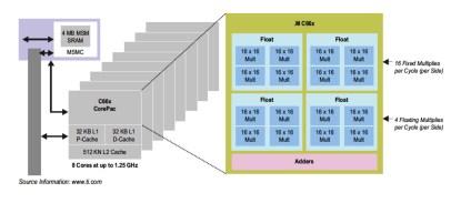
TMS320C667x DSP architecture.
DSPs, GPUs, and FPGAs serve as accelerators for many CPUs, providing both performance and power efficiency benefits. Given the variety of computing architectures available, designers need a uniform method to compare performance and power efficiency. The accepted method is to measure floating-point operations per second (FLOPs), where a FLOP is defined as either an addition or multiplication of single (32 bit) or double (64 bit) precision numbers in conformance with the IEEE 754 standard. All higher-order functions, such as division, square root, and trigonometric operators, can be constructed using adders and multipliers. As these operators, as well as other common functions such as fast Fourier transforms (FFTs) and matrix operators, require both adders and multipliers. There is commonly a 1:1 ratio of adders and multipliers in all these architectures.
Let's look at how we go about comparing the performance of the DSP, GPU, and FPGA architectures based on their peak FLOPS rating. The peak FLOPS rating is determined by multiplying the sum of the adders and multipliers by the maximum operation frequency. This represents the theoretical limit for computations, which can never be achieved in practice, since it is generally not possible to implement useful algorithms that can keep all the computational units occupied all the time. It does however provide a useful comparison metric.
First, we consider DSP GFLOPS performance. For this we selected an example device such as Texas Instruments' TMS320C667x DSP. This DSP contains eight DSP cores, with each core containing two processing subsystems. Each subsystem contains four single-precision floating-point adders and four single-precision floating-point multipliers. This is a total of 64 adders and 64 multipliers. The fastest version available runs at 1.25 GHz, providing a peak of 160 GigaFLOPs (GFLOPs).
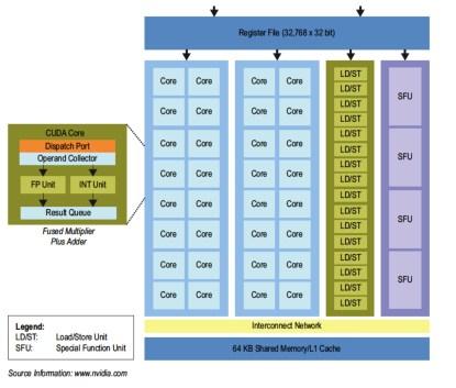
GPUs have become very popular devices, particularly for image processing applications. One the most powerful GPUs is the Nvidia Tesla K20. This GPU is based upon CUDA cores, each with a single floating-point multiple-adder unit that can execute one per clock cycle in single-precision floating-point configuration. There are 192 CUDA cores in each Streaming Multiprocessor (SMX) processing engine. The K20 actually contains 15 SMX engines, although only 13 are available (due to process yield issues, for example). This gives a total of 2,496 available CUDA cores, with two FLOPs per clock cycle, running at a maximum of 706 MHz. This provides a peak single-precision floating-point performance of 3,520 GFLOPs.

GP-GPU architecture.
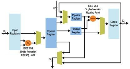
FPGA vendors such as Altera now offer hardened floating-point engines in their FPGAs. A single-precision floating-point multiplier and adder have been incorporated into the hard DSP blocks embedded throughout the programmable logic structures. A medium-sized FPGA, in Altera's midrange Arria 10 FPGA family, is the 10AX066. This device has 1,678 DSP blocks, each of which can perform two FLOPs per clock cycle, resulting in 3,376 FLOPs each clock cycle. At a rated speed of 450 MHz (for floating point -- the fixed-point modes are higher), this provides for 1,520 GFLOPs. Computed in a similar fashion, Altera states 10,000 GFLOPs, or 10 TeraFLOPs, of single-precision performance will be available in the high-end Stratix 10 FPGAs, achieved with a combination of both clock rate increases and larger devices with much more DSP computing resources.

Floating-point DSP block architecture in FPGAs.
Floating point routines have always been available in FPGAs using the programmable logic of the FPGA. Furthermore, with programmable logic-based floating point, an arbitrary precision level can be implemented that is not restricted to industry-standard single and double precision. For example, Altera offers seven different levels of floating-point precision. However, determining the peak floating-point performance of a given FPGA using a programmable logic implementation is not at all straightforward.
Therefore, the peak floating-point rating of any Altera FPGA is based solely on the capability of the hardened floating-point engines, and assumes that the programmable logic is not used for floating point, but rather for the other parts of a design, such as the data control and scheduling circuits, I/O interfaces, internal and external memory interfaces, and other required functionality.
There are several factors that make the calculation of floating-point performance using programmable logic very difficult. The amount of logic to build one single-precision floating-point multiplier and adder can be determined by consulting the FPGA vendor's floating-point intellectual property (IP) user guide. However, one vital piece of information is not reported in the user guide, and that is the routing resources required. To implement floating-point, large barrel shifters, which happen to consume tremendous amounts of the programmable routing (interconnect between the programmable logic elements) are required. All FPGAs have a given amount of interconnect to support the logic, which is based on what a typical fixed-point FPGA design will use.
Unfortunately, floating point does require a much higher degree of this interconnect than most fixed-point designs. When a single instance of a floating-point function is created, it can draw upon routing resources in the general region of the logic elements used.
However, when large numbers of floating-point operators are packed together, the result is routing congestion. This causes a large reduction in achievable design clock rates and logic usage that is much higher than a comparable fixed-point FPGA design. Altera has a proprietary synthesis technique known as "fused datapath," which does mitigate this to some extent, thereby allowing very large floating-point designs to be implemented in the logic fabric and leveraging fixed-point 27x27 multipliers for single precision, or 54x54 for double precision.
In addition, the FPGA logic cannot be fully used. Since the design takes up a large percentage of the available logic resources, the clock rate or fMAX at which timing closure can be achieved is reduced, and eventually timing closure cannot be achieved at all. Typically, 70% to 90% of the logic can actually be used and -- with dense floating-point designs -- it tends to be at the lower end of this range.
For all of the above reasons, it is nearly impossible to calculate the floating-point capacity of an FPGA when implemented in programmable logic. Instead, the best method is to build benchmark floating-point designs, which include the timing closure process. Alternatively, the FPGA vendor can supply such designs, which would greatly aid in estimating what is possible in a given FPGA.
Again, for example, Altera provides benchmark designs on 28nm FPGAs, which cover basic as well as complex floating-point designs. The published results show that with 28nm FPGAs, several hundred GFLOPs can be achieved for simpler algorithms such as FFTs, and just over 100 GFLOPs for complex algorithms such as QR and Cholesky decomposition.
Conclusion
FPGAs with hardened floating-point DSP blocks are now available, and provide single-precision performance from 160 to 1,500 GFLOPs in midrange devices, and up to 10,000 GFLOPs in high-end devices such as Altera's Stratix devices. These peak GFLOPs metrics are computed based on the same transparent methodology used on CPUs, GPUs, and DSPs.
This methodology provides designers a reliable technique for the baseline comparison of the peak floating-point computing capabilities of devices with very different architectures. The next level of comparison should be based on representative benchmark designs implemented on the platform of interest. For FPGAs lacking hard floating-point circuits, using the vendor-calculated theoretical GFLOPs numbers is quite unreliable. Any FPGA floating-point claims based on a logic implementation at over 500 GFLOPs should be viewed with a high level of skepticism. In this case, a representative benchmark design implementation is essential to make a comparative judgment. The FPGA compilation report showing logic, memory, and other resources, along with the achieved clock rate, should also be provided.
Michael Parker is Principal DSP Product Planning Manager at Altera.
| }
|